
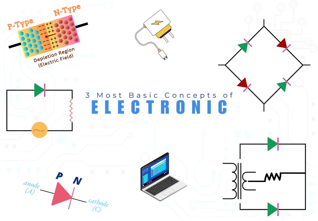
The 3 most basic concepts of electronics are at the heart of semiconductor devices like diodes, transistors, LEDs, and solar cells.
Table of Contents
Introduction
Have you ever wondered how a radio receiver extracts clear audio from a signal or how a phone charger converts high-voltage AC to the precise DC needed to charge your device? The answers lie in the behaviour of PN-junctions under biasing and the process of rectification.
The behaviour of PN-junction under forward and reverse bias forms the basis of isolating signals, as seen in a radio receiver, where it helps separate audio from carrier waves.
In a mobile charger, these principles enable converting high-voltage AC to low-voltage DC, ensuring safe and efficient power delivery to your phone battery.
Through understanding PN-junctions, biasing, and rectification, we unlock the foundational knowledge behind countless electronic devices and systems. In an electronic circuit, there are multiple components involved, such as capacitor, resistor, transformer, etc. But the main focus of study lies on the semiconductor diodes.
What is Electronics?
It is defined as,
“the branch of physics and engineering that deals with the study and application of devices that control the flow of electrons or charged particles.”
It enables the design of systems for communication, computation, and automation.
Basic Concept of Electronics
Modern electronics is built on three foundational concepts: the PN-junction, biasing, and rectification.
What is a diode?
A diode is a device that is made by joining two extrinsic semiconductor (p-type and n-type semiconductor) materials.
How it works
When the anode voltage (P-type) is higher than the cathode voltage (N-type), the diode is forward biased and current flows from the anode to the cathode. When the anode voltage is lower than the cathode voltage, the diode is reverse biased and no current flows.
1. PN-Junction
A PN-junction is created when a P-type semiconductor (which has an excess of holes or positive charge carriers) is joined with an N-type semiconductor (which has an excess of electrons or negative charge carriers).
This junction exhibits unique electrical characteristics that play a pivotal role in rectifying AC signals, controlling current, and enabling the functionality of various electronic components.
Key Terms to Understand PN-Junction in Action
Before proceeding into the working of the PN-junction, let us define some important terms that are often used when discussing its behaviour.
i. Depletion Region
The depletion region is the area around the PN-junction where the mobile charge carriers (electrons and holes) have diffused across the junction and recombined.
This region is devoid of any free-charge carriers, creating an insulating zone that prevents current flow under certain conditions.
ii. Potential Barrier
The potential barrier refers to the energy barrier created across the depletion region of the PN-junction. It is the result of the electric field that forms due to the diffusion of charge carriers between the P-type and N-type materials.
This barrier prevents the flow of current unless sufficient voltage (the threshold voltage) is applied to overcome it.
iii. Threshold Voltage
The threshold voltage (or cut-in voltage) is the minimum voltage that must be applied across the PN-junction in forward bias to reduce the potential barrier and allow significant current to flow.
For silicon diodes, this voltage is typically around 0.7V, while for germanium diodes, it is about 0.3V.
iv. Breakdown Voltage
The breakdown voltage is the reverse voltage at which the PN-junction undergoes breakdown. In such a case the current flows in the reverse direction.
When the reverse bias exceeds this voltage, the insulating properties of the junction break down, leading to a large reverse current. This phenomenon is often used in Zener diodes for voltage regulation.
v. Ripple Factor
The ripple factor is a measure of the smoothness of the output DC signal after rectification. It is defined as,
“the ratio of the AC component of the output signal to the DC component.”
A high ripple factor indicates a more pulsating output, while a low ripple factor means the output is closer to a pure DC signal. For half-wave rectification, the ripple factor is higher than for full-wave rectification, as the latter produces a smoother output.
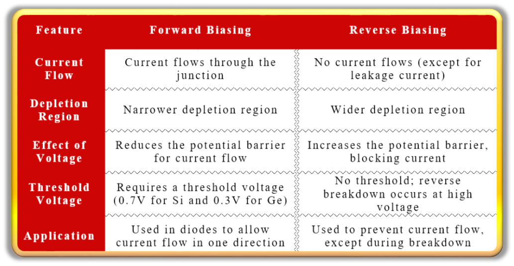
2. Forward Biasing and Reverse Biasing of a PN-Junction
The behaviour of a PN-junction can be analysed under two conditions:
- forward biasing
- reverse biasing
These two scenarios result in distinct electrical characteristics and play a critical role in devices such as diodes, which allow current to flow only in one direction.
Forward Biasing
When the positive terminal of the external power supply is connected to the P-type material and the negative terminal to the N-type material, the junction is said to be under forward bias.
- Width of Depletion Region: In this case, the external voltage reduces the width of the depletion region (the region where no charge carriers are present), allowing current to flow through the junction.
- Current Flow: In forward bias, the applied voltage causes the electrons in the N-type material to move toward the P-type material, and the holes in the P-type material to move toward the N-type material, leading to current flow.
- Threshold Voltage: For a silicon diode, a voltage of approximately 0.7V is required to overcome the potential barrier and allow significant current to pass. For a germanium diode, this threshold is around 0.3V.
Reverse Biasing
When the positive terminal of the external power supply is connected to the N-type material and the negative terminal to the P-type material, the junction is under reverse bias.
- Width of Depletion Region: In this case, the external voltage increases the width of the depletion region, preventing the flow of current. Only a small reverse leakage current may flow due to thermally generated charge carriers.
- Current Flow: Ideally, no current flows under reverse bias (except for a tiny leakage current). The reverse bias creates a larger depletion region, which acts as an insulator.
- Breakdown Voltage: If the reverse voltage exceeds a certain value (known as the reverse breakdown voltage), the junction may break down and allow a large current to flow in the reverse direction, potentially damaging the junction.
Forward Biasing vs. Reverse Biasing
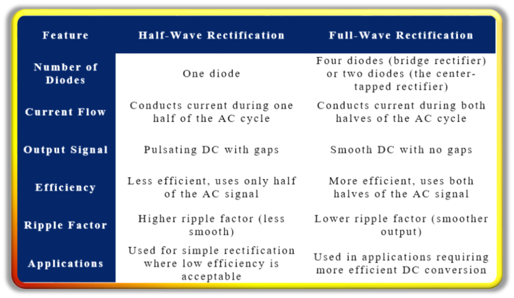
3. Half-Wave Rectification and Full-Wave Rectification
The ability of the PN-junction to conduct current only in one direction makes it ideal for rectification. Rectification is defined as,
“the process of converting alternating current (AC) into direct current (DC).”
There are two common types of rectification circuits and these are half-wave rectification and full-wave rectification.
Half-Wave Rectification
In half-wave rectification, a single diode is used to allow current to pass during only one half of the AC cycle (positive or negative). During the other half of the cycle, the diode is reverse-biased and blocks current flow.
- Operation: The diode conducts during the positive half-cycle when forward-biased, allowing current to flow. During the negative half-cycle, the diode is reverse biased, and no current flows.
- Output: The output of a half-wave rectifier is a pulsating DC signal, which is less efficient because only half of the AC waveform is used.
Full-Wave Rectification
In full-wave rectification, two diodes are used in a bridge configuration to rectify both halves of the AC cycle. The diodes work alternately, allowing current to pass in both the positive and negative cycles of the input signal.
- Operation: The first diode conducts during the positive half-cycle, while the second diode conducts during the negative half-cycle, both allowing current to flow in the same direction.
- Output: The result is a smoother DC output, as both halves of the AC waveform are utilised.
Half-Wave Rectification vs. Full-Wave Rectification
Conclusion
The PN-junction is a crucial component in the world of electronics, acting as a one-way valve for current flow in devices such as diodes.
Understanding the behaviour of a PN-junction under forward and reverse biasing is essential for appreciating its role in rectification.
Half-wave and full-wave rectification are two practical applications of PN-junctions that convert AC into DC, with full-wave rectification offering greater efficiency and smoother output.
By understanding these basic principles and key terms, one can better appreciate the underlying mechanics of various electronic devices and circuits. They lay the foundation for more advanced studies in electronics and semiconductor technology.
Frequently Asked Questions (FAQs)
What are the 3 most basic concepts of electronics?
The 3 most fundamental concepts are: the PN-junction, biasing, and rectification.
What is a PN junction in electronics?
A PN-junction is formed when a P-type semiconductor (rich in positive charge carriers or holes) is joined with an N-type semiconductor (rich in electrons or negative charge carriers). It plays a vital role in rectifying signals and controlling current in electronic devices.
What is the depletion region in a PN junction?
The depletion region is the area around the PN junction where mobile charge carriers have diffused and recombined, leaving behind an insulating zone devoid of free charge carriers.
What is the purpose of the potential barrier in a PN junction?
The potential barrier prevents current flow through the junction unless a sufficient external voltage is applied to overcome it. This barrier is due to the electric field formed by the diffusion of charge carriers.
How does forward biasing affect a PN junction?
In forward biasing, the depletion region’s width decreases as the external voltage reduces the potential barrier, allowing current to flow through the junction.
What happens during the reverse biasing of a PN junction?
In reverse biasing, the external voltage increases the depletion region’s width, preventing significant current flow. A small leakage current may occur due to thermally generated charge carriers.
What is rectification, and why is it important?
Rectification is the process of converting alternating current (AC) into direct current (DC). It is crucial for powering electronic devices that require a steady DC voltage, such as mobile chargers.
What is the difference between half-wave and full-wave rectification?
- Half-wave rectification uses a single diode to convert one-half of the AC cycle into DC, resulting in a pulsating output.
- Full-wave rectification uses two diodes in a bridge configuration to convert both halves of the AC cycle into DC, producing a smoother output.
What is the ripple factor, and why is it significant?
The ripple factor is the ratio of the AC component to the DC component in the rectifier output. A lower ripple factor indicates a smoother DC output, which is desirable for efficient power supply.
What is the breakdown voltage in a PN junction?
Breakdown voltage is the reverse voltage at which a PN-junction allows a large reverse current to flow, often leading to junction damage. Zener diodes leverage this phenomenon for voltage regulation.
Why is the threshold voltage important in forward biasing?
The threshold voltage is the minimum voltage needed to overcome the potential barrier in a forward-biased PN junction. For example, silicon diodes typically require 0.7V, while germanium diodes need around 0.3V.